Understanding Modern FPGA Design: From Silicon to Systems
A Comprehensive Analysis of Configurable Logic Systems and Their Building Blocks
Field-Programmable Gate Arrays (FPGAs) represent a remarkable achievement in digital electronics, offering the flexibility of programmable hardware with performance approaching that of custom-designed circuits. This article explores the intricate architecture of FPGAs, breaking down their fundamental components and operational principles.
Core Architecture Overview
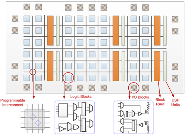
At its heart, an FPGA's architecture resembles a sophisticated electronic mosaic. Imagine thousands of tiny computational units arranged in a grid pattern, connected by a network of programmable wires – much like a city's streets connecting blocks of buildings. This basic structure consists of three primary elements:
Configurable Logic Blocks (CLBs) - the computational powerhouses
Programmable Interconnect Fabric - the communication network
Input/Output (I/O) Blocks - the interface with the external world
Configurable Logic Blocks: The Building Blocks
Configurable Logic Blocks, sometimes called Logic Elements (LEs) or Logic Cells (LCs), form the fundamental processing units of an FPGA. Think of each CLB as a miniature computational workshop, equipped with various tools to perform logical operations.
Key Components of a CLB
Look-Up Tables (LUTs)
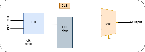
The cornerstone of each CLB is the Look-Up Table. A LUT functions like a pre-programmed reference guide, storing the outputs for every possible combination of inputs. Modern FPGAs typically employ LUTs that can handle four to six input bits. In our example architecture, the CLB uses two 3-input LUTs that can be combined to form a larger 4-input LUT, offering flexibility in implementation.
Full Adder (FA)
The Full Adder component enables arithmetic operations within the CLB. It can combine inputs from the LUTs with carry signals from adjacent CLBs, allowing the creation of larger arithmetic circuits like counters and multipliers.
D Flip-Flop (DFF)
The D Flip-Flop provides sequential logic capabilities, allowing the CLB to store and synchronize data with the system clock. This temporal element is crucial for creating sequential circuits and maintaining proper timing relationships.
Multiplexers (MUX)
Several multiplexers within the CLB act as configurable switches, determining the data flow path through the block. For example:
MUX 2 enables the combination of two 3-input LUTs into a single 4-input LUT
MUX 4 selects between FA output and LUT output
MUX 6 chooses between synchronous (clocked) and asynchronous operation
Operational Modes
A typical CLB supports multiple operational modes to accommodate different computational needs:
Normal Mode: The LUTs operate independently or combine to form larger lookup tables, ideal for complex combinational logic.
Arithmetic Mode: The full adder becomes active, accepting inputs from the LUTs and carry signals for mathematical operations.
The Interconnect Fabric: Bringing It All Together
The programmable interconnect fabric serves as the FPGA's nervous system, providing configurable routing between CLBs. This network consists of:
Horizontal and vertical routing channels
Programmable switches at channel intersections
Dedicated fast paths for carry chains in arithmetic operations
Input/Output Blocks: The Interface Layer
I/O blocks form the FPGA's interface with external devices, managing:
Voltage level translation
Signal buffering
Timing synchronization
Various I/O standards support
Modern FPGA Enhancements
Contemporary FPGAs have evolved beyond this basic architecture to include:
Dedicated DSP blocks for efficient signal processing
Embedded memory blocks
High-speed transceivers
Integrated microprocessor cores
Specialized blocks for AI acceleration
Programming and Configuration
The FPGA's configuration determines how each component behaves and interconnects. This involves:
Programming LUT contents
Setting multiplexer selections
Configuring routing paths
Establishing I/O parameters
The entire configuration is typically stored in on-chip memory, loaded at power-up from external non-volatile storage.
Practical Applications
This flexible architecture enables FPGAs to excel in various applications:
Digital signal processing
Custom processor design
Hardware acceleration
Prototyping of ASIC designs
Real-time systems
High-performance computing
Understanding this architecture is crucial for efficiently utilizing FPGAs in practical applications. The interplay between CLBs, routing resources, and specialized blocks provides the foundation for implementing complex digital systems while maintaining the flexibility to modify designs as needed.


